Texas Instruments - Texas Instruments

CDCDB800RSLR

HKD $102

8-output clock buffer for PCIe® Gen 1 to Gen 6

Features for the CDCDB800

  • 8 LP-HCSL outputs with programmable integrated 85-Ω (default) or 100-Ω differential output terminations
  • 8 hardware output enable (OE#) controls
  • Additive phase jitter after PCIE Gen 6 filter: 20 fs, RMS (maximum)
  • Additive phase jitter after PCIE Gen 5 filter: 25 fs, RMS (maximum)
  • Additive phase jitter after DB2000Q filter: 38 fs, RMS (maximum)
  • Supports Common Clock (CC) and Individual Reference (IR) architectures
    • Spread spectrum-compatible
  • Output-to-output skew: < 50 ps
  • Input-to-output delay: < 3 ns
  • Fail-safe input

  • Programmable output slew rate control

  • 3.3-V core and IO supply voltages
  • Hardware-controlled low power mode (PD#)
  • Current consumption: 72 mA maximum
  • 6-mm × 6-mm, 48-pin VQFN package

Description for the CDCDB800

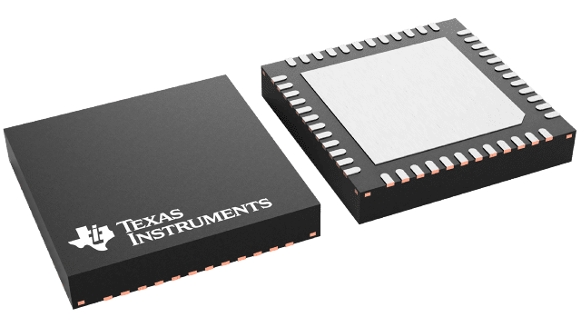
The CDCDB800 is a 8-output LP-HCSL, DB800ZL-compliant, clock buffer capable of distributing the reference clock for PCIe Gen 1-6, QuickPath Interconnect (QPI), UPI, SAS, and SATA interfaces. The SMBus interface and eight output enable pins allow the configuration and control of all eight outputs individually. The CDCDB800 is a DB800ZL derivative buffer and meets or exceeds the system parameters in the DB800ZL specification. It also meets or exceeds the parameters in the DB2000Q specification. The CDCDB800 is packaged in a 6-mm × 6-mm, 48-pin VQFN package.

購物與服務優勢

從線上下單到出貨與金流,我們以穩定交期與安全流程,協助您放心備料。

效率・交期彈性

採少量多樣計價與快速報價機制,搭配自有電子料倉, 支援急單需求,最快 24 小時即可交貨。

IC 現貨快速出貨

庫存料號下單後優先處理,可搭配分批出貨與 不同收貨地點,縮短開發與備料時間。

安心第三方支付

支援多家第三方支付與信用卡,全程加密處理交易, 不保留卡號資訊,金流與資料安全有保障。